Exposure systems use light to accurately transfer patterns onto materials or substrates.
It is essential in manufacturing semiconductors, printed circuit boards, displays, and MEMS, enabling high-precision processing.
Our exposure systems deliver high precision and efficiency, supporting everything from prototyping to mass production, helping customers enhance productivity and quality.
State of the art ADTEC Exposure Systems
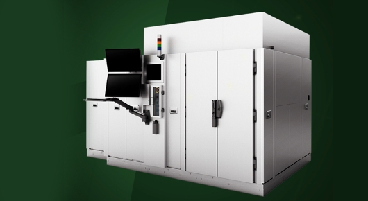
In the advanced package area, even higher definition wiring formation is required. Starting with the production of substrates, ADTEC Engineering offers optimal solutions in combination with direct-imaging exposure systems for semiconductor back-end processes, which we were the first to introduce to the market, in addition to an expansion of models for the high-definition area.
A wide range of lineup for IC-substrate production, high multilayer boards, and various printed circuit boards.
Maskless direct-imaging exposure systems using laser diodes and contact exposure systems, etc., meet the resolution requirements of production products and the materials to be used.
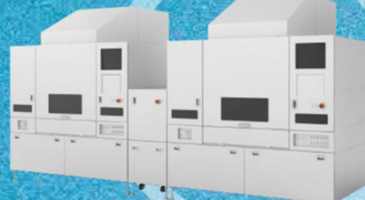
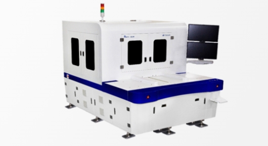
INPREX IP-4 V2 for high-performance IC package substrates.IP-6 SW for a wide range of applications from high-definition to HDI. IP-15 UHT, which specializes in productivity, is available in a wide range of products.
Combined with h-line wavelength DFR, INPREX offers maximum productivity and exposure imaging performance. Automatic transfer of various substrate sizes, from conventional standard substrate sizes to large, thick, and heavy substrates, has been realized.
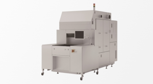
ADEX is a standard fully automated exposure system that uses masks. We have double-sided simultaneous exposure systems that excel in productivity, as well as contact-type exposure systems in upstream and downstream line configurations for both pattern formation and solder resist.
Second-hand Equipment
DMD type maskless exposure system that eliminates the need for photomask management.
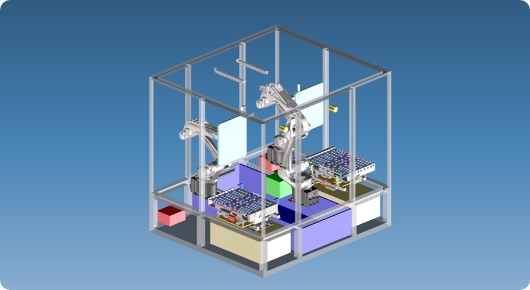
Applicable to semiconductor back-end process applications such as circuit formation on package substrates, via formation on insulating layers, and Redistribution layer lithography.
From FO-WLP-Wafer to PLP-Panel Size.
Direct-Imaging Exposure for high-definition package substrates and high-definition, multilayer substrates.
Please check ADTEC PCB production related systems.
Following systems and equipment are helpful for PCB production.
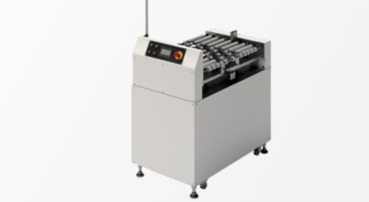
Equipment that automatically peels off protective films of various film materials DFR (dry film photoresist), interlayer insulating materials, DFSR (dry film solder resist), polyimide films, etc. in the substrate manufacturing process.
PAVIS-LV Series
Inspects for smear (residue) after de-smear process, which causes via cracks after via formation.
Also automatically inspects all LVH on the panel surface and accurately detects them with our unique patented technologies.
AKC Co., Ltd. is responsible for design and manufacturing, and ADTEC is responsible for sales and maintenance service in Japan.
Enables adjustment of adsorption conveyor adsorption force Adjust to optimum setting for board transport A simple dry cleaner with just cyclone brush and dirt suction.
Double-sided alignment marking system for inner layer patterning
AMRK1000(for Standard) / AMRK2000(for Large Size Panels)
This system forms fiducial marks by UV exposure, on the DFR of inner layer panels without through holes. To eliminates the need for reference hole processing.