Printed Circuit Boards (PCBs) are crucial components that serve as the heart of electronic devices. As the demand for higher density and precision increases, the manufacturing process requires advanced technology. Our company contributes to improving the quality of PCB production by utilizing precise exposure technology. On this page, we introduce a step in the PCB manufacturing process to provide a reference for how they are made.
Process5
Resist Stripping
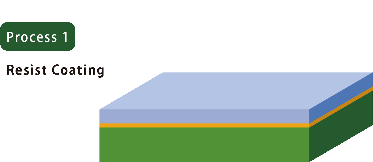
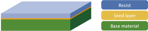
Process1
Resist Coating
This section introduces the process of creating printed circuit boards. The patterning process is the process of forming conductive wiring on a printed circuit board.
What is dry film resist?
Dry film resist (DFR) is a photosensitive covered film that cures the exposed area.
What kind of material is the base material ?
Substrates are made of organic materials such as paper, glass cloth, and resin, or inorganic materials such as glass, and are reinforcing materials for laminating and encapsulating printed circuit boards and semiconductor chips.
Process2
Exposure
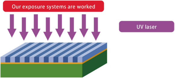
Prepare circuit pattern data to be drawn on the surface of photosensitive resist film.
The circuit pattern is irradiated and exposed by UV light from laser diode.
I've heard of UV light…
UV light is ultraviolet light. It uses a special wavelength of light that is not normal light (visible light).
What do you mean by “expose”?
Exposure is the process of sensitizing and curing the resist surface by exposing it to the light of the circuit pattern.
What is the circuit pattern data to be drawn?
It is data of wiring circuits to be installed on a printed circuit board, with wiring conductors represented in green and black.
It is also called Gerber data.
Exposure Systems
Process3
Developing
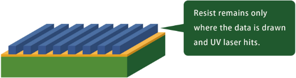
After “exposure,” the resist cures in the areas exposed to light and does not cure in the areas not exposed (unexposed areas). The unexposed areas are placed in a special solvent to remove the resist. This is called developing.
Is developing film the same as developing a photograph?
Developing is the process of leaving the areas exposed to UV light and removing the remainder. The principle is the same as that of photographic development.
I've never heard the word “resist” before…
Resist is a protective coating material used to protect the copper foil necessary to form conductive wiring.
Process4
Copper Plating

In the additive process, the seed layer is primed and copper plated.
This creates a new base for plated wiring on the substrate.
What is an additive process?
The additive process is more suitable for producing finer wiring than using the copper foil portion of conventional copper clad laminates as wiring.
What is a seed layer?
A plating substrate is laid down in advance on the area to be plated.
The plating will bond to this to form finer and more solid wiring.
Process5
Resist Stripping
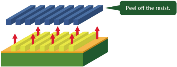
The resist is peeled off to expose the originally laid seed layer.
How do you peel off the resist?
Resist stripping is performed using a chemical solvent or other means.
Process6
Flash Etching
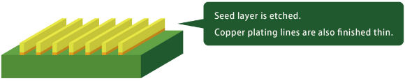
Unnecessary seed layers are removed.
In doing so, the plating is likewise removed, but this also polishes the newly formed wiring and forms it into a better shape.
Does etching mean scraping?
Etching is a method of chemically removing unwanted copper on a plate.
How do you remove the seed layer?
It uses a surface finishing technique that applies a corrosive action with chemicals.
Let's look at process 1.
Process 1 through Process 6 are shown in the animation.